P – N Junction Diode
A P-N Junction Diode is formed by doping one side of a piece of silicon with a P-type dopant and the other side with an N-type dopant. Ge can be used instead of Silicon. The P-N junction diode is a two terminal device. This is the basic construction of the P-N junction diode. It is one of the simplest semiconductor devices as it allows current to flow in only one direction. The diode does not behave linearly with respect to the applied voltage, and it has an exponential V-I relationship.
What is a P – N Junction Diode?
A P – N junction diode is a piece of silicon that has two terminals. One of the terminals is doped with P – type material and the other with N-type material. The P-N junction is the basic element for semiconductor diodes. A Semiconductor diode facilitates the flow of electrons completely in one direction only – which is the main function of semiconductor diode. It can also be used as a Rectifier.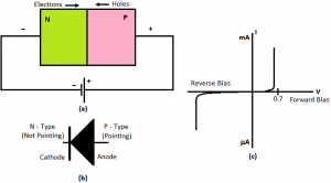 P – N Junction Diode Theory: There are two operating regions: P-type and N-type. And based on the applied voltage, there are three possible “biasing” conditions for the P-N Junction Diode, which are as follows:
Zero Bias: No external voltage is applied to the PN junction diode.
Forward Bias: The voltage potential is connected positively to the P-type terminal and negatively to the N-type terminal of the Diode.
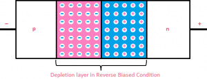
Reverse Bias: The voltage potential is connected negatively to the P-type terminal and positively to the N-type terminal of the Diode.
Zero Biased Condition: In this case, no external voltage is applied to the P-N junction diode; and therefore, the electrons diffuse to the P-side and simultaneously holes diffuse towards the N – side through the junction, and then combine with each other. Due to this an electric field is generated by these charge carriers. Electric field opposes further diffusion of charged carriers so that there is no movement in the middle region. This region is known as depletion width or space charge.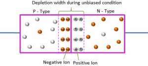 Forward Bias: In the forward bias condition, the negative terminal of the battery is connected to the N – type material and the positive terminal of the battery is connected to the P-Type material. This connection is also called as giving positive voltage. Electrons from the N – region crosses the junction and enters the P – region. Due to the attractive force that is generated in the P – region the electrons are attracted and move towards the positive terminal. Simultaneously the holes are attracted towards the negative terminal of the battery. By the movement of electrons and holes current flows. In this condition, the width of the depletion region decreases due to the reduction in the number of positive and negative ions.
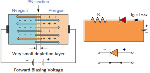 Reverse Bias: In the forward bias condition, the negative terminal of the battery is connected to the N-type material and the positive terminal of the battery is connected to the P-type material. This connection is also known as giving positive voltage. Hence, the electric field due to both the voltage and depletion layer is in the same direction. This makes the electric field stronger than before. Due to this strong electric field, electrons and holes want more energy to cross the junction so they cannot diffuse to opposite region. Hence, there is no current flow due to lack of movement of electrons and holes.